I specialize in VLSI front-end design and verification. I have hands-on experience in Verilog, SystemVerilog, UVM, and am comfortable working with Cygwin, GVim, and QuestaSim in real-world verification environments. I’ve built and verified FIFO, RAM, AHB Lite, and DMA controller projects, and am currently part of the XCHIP Cohort SMP. Passionate about semiconductor tech, CPUs, GPUs, and automotive engineering. Always learning, always building!
Interests: VLSI Design & Verification, Programming and Automation, Latest Tech Trends, Automobile Engineering and Car Tuning
Selected projects
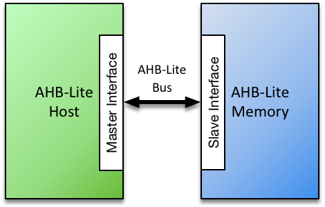
AHB Lite Protocol
The module adheres to the AMBA 3 AHB-Lite standard, optimized for single-master configurations, as frequently used in microcontrollers and embedded systems. It features a full range of burst capabilities—fixed-length (INCR4, INCR8, INCR16) and variable-length INCR-mode bursts—and implements automatic pipelining with HTRANS, HBURST, HSIZE, and HREADY protocol signals.
SystemVerilogUVMQuestaSim
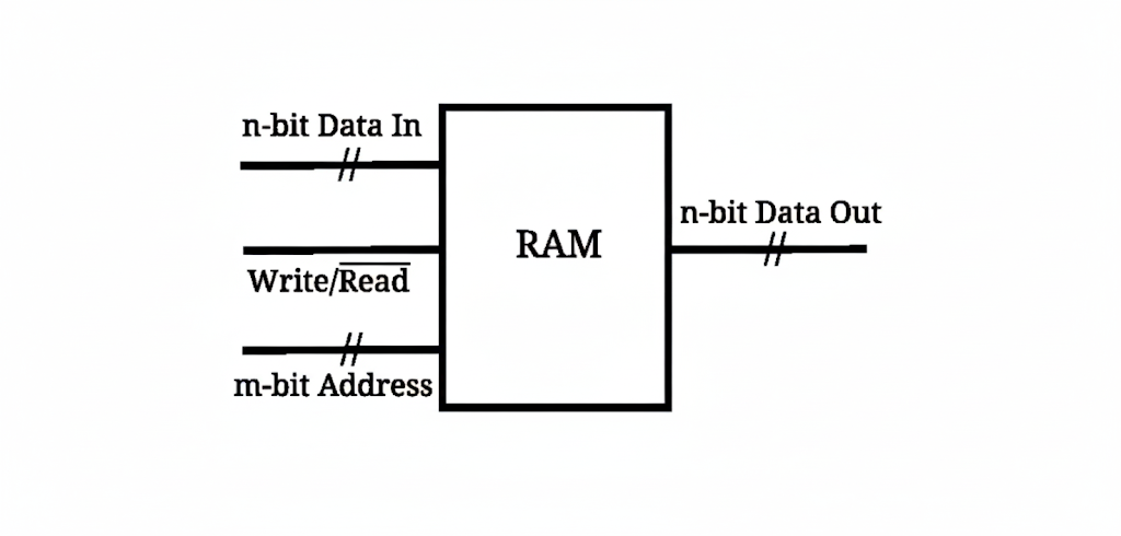
Successfully completed my first UVM-based verification project by designing and verifying a 64KB asynchronous RAM. This was a hands-on dive into UVM testbench development, with a deliberately simple DUT to help focus on building a robust verification environment from scratch. Developed a fully functional UVM testbench with 7 custom sequences and 4 test cases to cover all DUT signal behaviors.
SystemVerilogUVMQuestasim
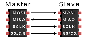
SPI MASTER Design
Built an SPI master module capable of generating accurate SCLK signals for all combinations of CPOL and CPHA, making it fully compliant with standard SPI modes. Clock generation is handled using a counter-based method to derive a lower-frequency SCLK from a high-frequency system clock. Dynamically supports all SPI modes through configurable CPOL and CPHA.
SystemVerilogEDA Playground
E2E SCB
Designed a configurable class-based packet generator supporting 3 traffic patterns:
1️⃣ All Same – identical addresses with varied data across instances
2️⃣ Two Same – 2 common addresses, rest unique
3️⃣ All Different – fully distinct address-data pairs across instances
Built an associative memory table to visualize and track data transactions per address across instances. Integrated test control via .do file to pass packet count (n) and added partial automation with a .sh script for batch runs.
SystemVerilogEDAQuestasim
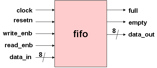
FIFO Modeling
Created a functional FIFO model to synchronize data between a fast transmitter and a slow receiver, using separate read and write clocks. This project focused on reliable data handling and control signal generation in asynchronous environments. Implemented a pointer-based FIFO with support for full, empty, overflow, and underflow status flags. FIFO memory structure: [7:0] mem [31:0] — 8-bit wide, 32-depth buffer. Verified functionality using a custom SystemVerilog testbench with constraints and randomizations.
SystemVerilogUVMQuestasim
Skills
Verilog85%
SystemVerilog90%
UVM88%
Simulation & STA85%
Digital Circuits88%
Analog Circuits75%
C Programming95%
Scripting75%
OOP Concepts85%
Experience & Education
Design and Verification Intern — Xchip Technologies
Jun 2025 — Present
Working on RISC V 32 core development and 3 Channeled DMA Controller with AHB Lite Bus.
Bachelor of Engineering (BE)
Sri Shakthi Institute of Engg and Technology • 2022-2026
Relevant coursework: Digital and Analog Electronics, VLSI Design, ASIC Flow.